



Key Takeaways
- NVIDIA and Applied Materials have developed an end-to-end digital model combining GPU-accelerated simulation and digital twins for semiconductor innovation.
- Performance gains include up to 55x speedups in quantum chemistry simulations and 35x faster chamber modeling, enabling rapid virtual exploration of materials and processes.
- The collaboration addresses growing complexity in chipmaking, with equipment spending projected to reach nearly $40 billion by 2031, as analyzed by Semiconductor Engineering.
Semiconductor Innovation at the Speed of AI: 55x Faster Simulation Unlocks Next-Gen Chips
As AI workloads drive explosive demand for compute, the semiconductor industry faces unprecedented pressure to deliver faster, more efficient chips. Traditional materials engineering and manufacturing approaches are too slow and costly to keep pace.
Now, a collaboration between Applied Materials and NVIDIA aims to change that with an end-to-end digital development model that unifies atomic-scale discovery, process engineering, and factory optimization. The platform leverages NVIDIA CUDA-X libraries to accelerate simulations, achieving up to 55x speedups in quantum chemistry and 35x faster chamber simulations, enabling engineers to explore materials and processes virtually before committing to physical experiments.
Table of Contents
Atomic-Scale Simulation Gets a GPU Boost
At the heart of the collaboration is Ginestra, a physics-based simulation platform from Applied Materials that links material properties and defects to device performance. Ginestra is designed to tackle the complexities of advanced 3D structures like gate-all-around transistors, where multiple materials are packed into nanometer-scale spaces.
Traditionally, achieving the required simulation fidelity required significant compute time. By integrating NVIDIA cuDSS, a GPU-accelerated sparse solver, Ginestra delivers up to 10x speedups over CPU-only approaches. For even more demanding quantum chemistry calculations, NVIDIA’s cuEST library accelerates density functional theory workflows, reducing simulation time from five days on 64 CPU cores to just two hours on a single GPU—a 55x improvement.
These speedups allow engineers to run thousands of virtual experiments across material combinations, dramatically expanding the pool of viable candidates and reducing reliance on costly physical trials.
Accelerating Process Engineering with Digital Twins
Once promising materials are identified, the next challenge is translating those insights into repeatable, high-yield manufacturing processes. The Applied Materials ACE+ platform brings together multiphysics models—fluid flow, heat transfer, plasma dynamics, and surface reactions—to simulate chamber and process behavior.
NVIDIA PhysicsNeMo converts these simulation results into real-time digital twins of process behavior. With GPU acceleration, ACE+ topography simulations run up to 35x faster, compressing workflows that once took days into same-day results. Engineers can dynamically explore parameter changes and see instant impact, shifting from batch-based iteration to a continuous, interactive workflow that converges on optimized conditions much earlier.
Validated process innovations are then deployed into production using platforms like Endura, the semiconductor industry’s most successful metallization system, which combines multiple process steps under vacuum.
Fab-Wide Optimization Through Virtual Environments
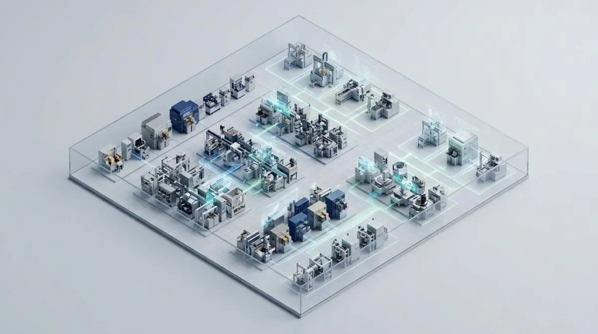
At the factory scale, Applied Materials leverages NVIDIA Omniverse libraries to build physically accurate digital twins of entire fabs. These virtual environments allow teams to optimize layouts, simulate material flow, identify bottlenecks, and validate operational strategies before deployment.
This digital thread—from atomic-scale simulation through process engineering to fab optimization—creates a continuous flow of insights that accelerates the innovation pipeline. According to the companies, this integrated approach is essential for meeting the growing compute demands of the AI era.
Strategic Implications for AI Hardware
This collaboration arrives at a critical time for the semiconductor industry. As process complexity compounds, particularly in areas like etch and deposition, equipment spending is projected to rise from the mid-$20 billion range today to nearly $40 billion by 2031, according to a recent analysis by Semiconductor Engineering. Feature-scale effects such as high-aspect-ratio etching and material-dependent reactions now directly determine profile control and yield.
The integration of digital twins and AI-enabled workflows is becoming essential for navigating this complexity. As noted in a recent Semiconductor Engineering blog, calibrated physical models combined with AI/ML and automation agents are helping process engineers explore wider process windows while maintaining trust in virtual predictions. The ultimate goal is to turn digital twins into everyday engineering decision-support tools.
For the AI industry, faster semiconductor innovation means more powerful hardware can reach the market sooner. The ability to virtually test materials and processes reduces the risk of costly delays in AI hardware cycles, where even small setbacks can have outsized financial impact. As the demand for specialized AI accelerators grows, the kind of end-to-end digital development model pioneered by NVIDIA and Applied Materials could become a competitive necessity.
The Future of Semiconductor Innovation
The collaboration between NVIDIA and Applied Materials represents a shift toward cross-ecosystem innovation in the semiconductor value chain. By combining leadership in materials engineering with GPU-accelerated simulation and digital twins, the two companies are creating a continuous digital thread that spans the entire innovation lifecycle, from atoms to fabs. This connected model will be critical for powering the next generation of AI infrastructure.
This kind of AI-driven simulation and optimization mirrors the work we do at Andres SEO Expert, where we help businesses leverage programmatic AI to streamline complex workflows and improve digital performance. If you’re interested in applying similar automation principles to your operations, explore our programmatic AI automation services. For more about our approach, visit Andres SEO Expert. To discuss your specific goals, connect with Andres.
Frequently Asked Questions
What is the 55x simulation speedup mentioned in the article?
The 55x speedup refers to quantum chemistry simulations using NVIDIA’s cuEST library, which reduced simulation time from five days on 64 CPU cores to just two hours on a single GPU. This acceleration enables engineers to run thousands of virtual experiments across material combinations.
Which companies are leading this semiconductor innovation collaboration?
Applied Materials and NVIDIA are collaborating to create an end-to-end digital development model for semiconductor manufacturing. Applied Materials provides physics-based simulation platforms like Ginestra and ACE+, while NVIDIA contributes GPU-accelerated libraries such as CUDA-X, cuDSS, cuEST, PhysicsNeMo, and Omniverse.
How do digital twins accelerate process engineering?
Digital twins, powered by NVIDIA PhysicsNeMo, convert multiphysics simulation results into real-time models of chamber and process behavior. With GPU acceleration, ACE+ topography simulations run up to 35x faster, compressing workflows from days to same-day results and enabling interactive parameter exploration.
What is the role of NVIDIA cuDSS in atomic-scale simulation?
NVIDIA cuDSS is a GPU-accelerated sparse solver integrated into Applied Materials’ Ginestra platform. It delivers up to 10x speedups over CPU-only approaches for physics-based simulations of advanced 3D transistor structures, linking material properties and defects to device performance.
How does this technology improve fab-wide optimization?
Applied Materials uses NVIDIA Omniverse libraries to create physically accurate digital twins of entire factories. These virtual environments allow teams to optimize layouts, simulate material flow, identify bottlenecks, and validate operational strategies before physical deployment, creating a continuous digital thread from atoms to fabs.
What are the strategic implications for AI hardware?
Faster semiconductor innovation means more powerful AI hardware can reach the market sooner. The ability to virtually test materials and processes reduces risk and delays in AI hardware cycles, which is critical as equipment spending for etch and deposition is projected to rise to nearly $40 billion by 2031.
How does this approach reduce reliance on physical experiments?
By enabling up to 55x faster simulations and interactive digital twins, engineers can run thousands of virtual experiments across material combinations and process parameters. This dramatically expands the pool of viable candidates and minimizes costly physical trials, accelerating the innovation pipeline.