



Key Takeaways
- NVHBM delivers up to 30% more memory bandwidth, 25% more compute die area, and 15% lower power for custom XPUs.
- NVLink Fusion integrates custom XPUs into NVIDIA’s NVLink fabric, enabling rack-scale heterogeneous AI factories.
- At fleet scale, reduced HBM power can free capacity for up to 15,000 additional XPUs in a gigawatt data center.
Table of Contents
Custom Chips Enter the NVIDIA AI Factory With a 30% Performance Jump
As of late August 2026, hyperscalers and AI-native companies have a tighter path to deploying custom XPUs inside NVIDIA’s AI infrastructure platform.
NVIDIA’s developer portal published the technical specification on August 26, 2026, and the headline numbers are aggressive: up to 30% higher memory bandwidth per stack, 25% more compute die area, and 15% lower HBM power usage compared with standard HBM4e.
Those three gains compound into roughly 30% better end-to-end XPU performance.
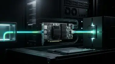
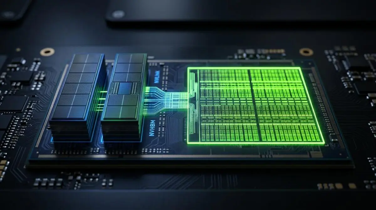
As detailed on NVIDIA’s developer blog, the architecture pairs NVLink Fusion, a chiplet-based connectivity layer, with NVHBM, a custom HBM base-die technology built alongside memory vendors.
Why Memory Bandwidth, Die Area, and Power Dominate Accelerator Design
Custom accelerator programs live or die on three physical constraints: memory bandwidth, usable die area, and power delivery.
NVLink Fusion and NVHBM address all three at the package level, which is where custom silicon decisions get locked in early.
- Up to 30% more memory bandwidth per stack compared with standard HBM4e
- Up to 25% more compute die area from a smaller PHY and integrated memory controller
- Up to 15% lower HBM power usage that cascades into rack and data center headroom
Memory bandwidth at the package level
HBM keeps model weights, KV cache data, and activations close to the accelerator.
NVHBM raises usable memory bandwidth by up to 30% per stack, which keeps compute cores fed during memory-bound training and inference phases.
For large-model token generation, that means faster data movement between HBM and compute, improving per-user throughput without requiring a wider package.
Reclaiming silicon area for specialized compute
Standard HBM interfaces use wider connections that consume interposer routing space and package area.
NVHBM uses a custom base die and PHY, moves the memory controller into the 3D HBM stack, and reduces the I/O area required to reach memory.
Compared with the JEDEC HBM4e standard, the redesigned PHY and support area shrink by up to 67%.
The narrower interface simplifies interposer routing and opens up to 80% more usable silicon across the layout.
That reclaimed space can expand the main compute die by up to 30%, giving XPU designers room for workload-specific accelerators, larger matrix engines, or additional on-chip memory.
Power headroom compounds at AI factory scale
NVHBM cuts HBM power usage by up to 15% compared with standard HBM4e.
At the XPU level, that creates thermal and power headroom for sustained compute utilization.
The effect becomes more visible at fleet scale.
In a one-gigawatt data center using 2,000-watt XPUs, the cumulative memory power savings can enable up to 15,000 additional XPUs in compute headroom.
What Rack-Scale XPU Integration Means for AI Factory Operators
NVLink Fusion extends the package-level gains into a rack-scale system.
Its chiplet bridges custom XPUs to the sixth-generation NVLink fabric, creating a single scale-up domain across GPUs, CPUs, and XPUs.
That coherence matters most for advanced routing techniques such as expert parallelism and WideEP.
When different experts sit on separate accelerators, the fabric moves activations and hidden states fast enough to keep distributed inference synchronized.
Upstream, NVLink-C2C connects the custom XPU to the CPU, so the accelerator does not have to operate as an isolated island.
NVLink Fusion adopters can also tap NVIDIA’s scale-up and scale-out stack, MGX rack architecture, and broader ecosystem.
This reduces development complexity and accelerates time to market for semi-custom AI factories.
The strategic payoff extends to operations: a unified fabric simplifies capacity reprovisioning and lets custom XPUs interoperate with NVIDIA GPUs for heterogeneous compute.
Meanwhile, NVHBM base dies validated with leading memory manufacturers reduce integration and qualification bottlenecks for accelerator teams.
Custom Silicon Gets a Direct Line to Production AI Infrastructure
NVLink Fusion and NVHBM collapse the distance between a custom accelerator design and production AI factory capacity. For teams building AI infrastructure narratives that need to dominate search with the same precision as a rack-scale fabric coordinates distributed compute, programmatic SEO and AI automation service is how Andres SEO Expert approaches it — contact us to shape yours.
Frequently Asked Questions
What are NVLink Fusion and NVHBM?
NVLink Fusion is a chiplet-based connectivity layer that connects custom XPUs to NVIDIA’s sixth-generation NVLink fabric. NVHBM is a custom HBM base-die technology built alongside memory vendors, offering higher memory bandwidth, more compute die area, and lower power usage compared with standard HBM4e.
How much performance improvement do custom chips get with NVHBM?
Custom chips can achieve up to 30% higher memory bandwidth per stack, 25% more compute die area, and 15% lower HBM power usage, compounding into roughly 30% better end-to-end XPU performance.
What physical constraints in custom accelerator design does NVIDIA’s new technology address?
The technology addresses memory bandwidth, usable die area, and power delivery at the package level. NVHBM increases memory bandwidth per stack, frees up silicon area by shrinking the PHY and integrating the memory controller, and reduces HBM power usage.
How does NVHBM increase memory bandwidth and reduce power?
NVHBM uses a custom base die and PHY that moves the memory controller into the 3D HBM stack, reducing I/O area and simplifying interposer routing. This yields up to 30% more memory bandwidth per stack, up to 80% more usable silicon, and up to 15% lower HBM power usage.
How does NVLink Fusion integrate custom XPUs into rack-scale AI infrastructure?
NVLink Fusion uses chiplet bridges to connect custom XPUs to the sixth-generation NVLink fabric, creating a single scale-up domain across GPUs, CPUs, and XPUs. This enables advanced routing techniques like expert parallelism and WideEP, and supports heterogeneous compute with NVIDIA GPUs.
What are the benefits of the custom base die and PHY in NVHBM?
The custom base die and PHY reduce the I/O area required for memory by up to 67%, simplify interposer routing, and open up to 80% more usable silicon. This allows the main compute die to expand by up to 30% for workload-specific accelerators or additional on-chip memory.
How does this technology affect AI factory operators?
AI factory operators benefit from lower memory power usage, enabling up to 15,000 additional XPUs in a one-gigawatt data center. The unified fabric simplifies capacity reprovisioning, reduces development complexity, and accelerates time to market for semi-custom AI factories.